IC Packaging
The presence of Integrated Circuits (ICs) in any project, confirms a revolution in the electronics world! Having said that, there’s no point in doubting ICs being called the cornerstones of state-of-the-art electronics.
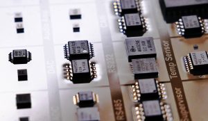
Packaging refers to objects being placed in a box. Here, IC packaging refers to the material containing the semiconductor devices, dimension,s, and shape of a chip. Even the chips containing the same electronics parameter may have different package types. The package is nothing but a casing that encompasses the circuit material to protect it from corrosion or physical damage. The pins of the IC package act as electrical contacts that are connected to PCB through soldering.
IC packages are mainly categorized into traditional DIP dual-in-line and SMD chip packages, they are soldered by different methods (Wave soldering & Reflow soldering).
There are varieties of integrated circuits and thus this brings varieties in types of IC packaging used depending on circuit designs, system design, and requirements of the outer shell.
After discussing the IC package definition, let us talk about different categories of IC packages:
Pin-grid array: Used for socketing.
Lead-frame and dual-inline packages: For assemblies in which pins go through holes. This package mounts to a circuit board with either a through-hole or a socket.
Chip scale package: Single-die, direct surface mountable package, with an area that’s smaller than 1.2 times the area of the die.
Quad flat pack: A lead-frame package of the leadless variety.
Quad flat no-lead: For surface-mounting A tiny package, the size of a chip, used for surface mounting.
Multichip package: Multichip packages, or multichip modules, integrate multiple ICs, discrete components and semiconductor die onto a substrate, making it so the multichip package resembles a larger IC.
Area array package: These packages offer maximum performance while still conserving space by allowing any portion of the chip’s surface area to be used for interconnection.
MOUNTING STYLE:
One of the major distinguishing characteristics of IC package type is the manner in which the components are mounted on the printed circuit board. All the packages fall into either of two types of mounting: Through-hole (PTH) or Surface-mount (SMD or SMT)
Through-hole packages are generally bigger, and easy to work with. They’re designed to be stuck through one side of a board and soldered to the other side.
Surface-mount packages range in size from small to minuscule. They are all designed to mount on one side of a circuit board and be soldered to the surface. ICs in this form factor is not easy to assemble manually. They usually require special tools to aid in the process.

THROUGH-HOLE PACKAGING
In PTH, the lead pins are inserted through one side of the board and soldered on the other. These are generally used in electronic equipment that does not demand compact board space and cost limitations. Dual inline packages (DIP) are the most common through-hole IC packages.
These little chips have two parallel rows of pins extending perpendicularly out on a black plastic housing which is rectangular in shape. The pins are spaced at 0.1 inches (2.54mm) which is a standard spacing and perfect for fitting into breadboards and other prototyping boards. The overall dimensions of a DIP package depend on its pin count, which may be anywhere from four to 64. The area between each row of pins is perfectly spaced to make sure they do not short to each other.
There are many types of DIP Packages: Plastic Dual In-Line Package (PDIP) and Molded Dual In-Line Package (MDIP) are the few popular types. Further, it can be classified as
Standard – This is the most common packaging. The pins are spaced 2.54mm (0.1”) apart. Skinny – In this packaging, the space between the terminal rows is 7.62mm.
Shrink – Similar to the standard ones but the lead pitch is 1.778 mm. Smaller in size, they use high pin density packaging.
Zig-Zag in Line Packages (ZIP)-The pins in this kind of package are inserted perpendicularly to the circuit board. These pins are perpendicularly aligned in the package and closer to each other. This sort of packaging was short-lived and was mainly used in dynamic RAM chips.
Surface Mount Packaging
Surface mount technology deals with mounting or placing the components directly on the surface of the printed circuit board. Although this process of fabrication helps do things quickly, it also increases the chances of defects, if assembled manually. The reason is the miniaturization of components and also because they are mounted extremely close to each other. This, in turn, results in making it extremely important to detect the failure in the entire process. Again, Surface mount packaging also uses ceramic or plastic molding.
The different types of surface mount packages that use plastic molds are as following:
Small outline L-leaded package- This type has gull-wing type leads that draw out in either direction from the body in an L fashion and can be mounted directly on the board.
Quad Flat L-leaded Packages (QFP) – These are similar to SOP. However, the only difference is that the leads are drawn out in 4 directions instead of 2 and are mounted directly on the board. They also come with a heat sink and built-in heat spreader.
Ball Grid Array (BGA) – These have solder ball arrays on the back surface of PCBs.
Fine Pitch Land Grid Array– These have solder land arrays on the back surface of PCBs.
Wafer Level Chip Size Package– Many Individual chips are made out of a packaged wafer that is cut out.


Leave a Reply